42 how to draw energy band diagram
https://www.patreon.com/edmundsjIf you want to see more of these videos, or would like to say thanks for this one, the best way you can do that is by becomin... https://www.patreon.com/edmundsjIf you want to see more of these videos, or would like to say thanks for this one, the best way you can do that is by becomin...
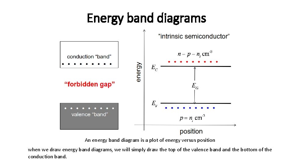
Energy band diagrams . Lundstrom: 2018 . An energy band diagram is a plot of the bottom of the conduction band and the top of the valence band vs. position. Energy band diagrams are a powerful tool for understanding semiconductor devices because they provide . qualitative solutions to the semiconductor equations.
How to draw energy band diagram
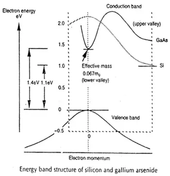
Pls draw the energy diagram when zero bias is applied to the top electrode. Homework Equations We are taught how to draw the energy diagram for a metal-oxide-semiconductor structure. In this question, we are asked to draw a SOS structure. The Attempt at a Solution Comrades, in this video, we learn about the fabrication of P-N diodes and the Energy band diagram (EBD) of P-N diodes. Here are the timestamps so that you ca... Energy Band Strucure of GaAs. For GaAs, the effective mass of these electrons is 0.067 times the mass of free electron (that is, 0.067m e, where m e is the free electron rest mass). Thus the shapes in the conduction band bring about a superior electron mobility. Due to this, the electrons travel faster in Gallium Arsenide (GaAs) than in Silicon.
How to draw energy band diagram. Hey Comrades! If you want to learn THE EASIEST METHOD to draw ANY Energy Band Diagram (EBD), then this video is a must-watch for you. I classified the 2 fact... 1) Energy band diagrams provide a qualitative understanding of how MOSFETs operate. 23 . 2) MOSFETs are barrier controlled devices - the drain current is controlled by the height of an energy barrier between the source and channel. Lundstrom: 2018 3) In a well-designed transistor, the height of the energy Semiconductor Device Modeling by Prof. S. Karmalkar,Department of Electrical Engineering,IIT Madras.For more details on NPTEL visit http://nptel.iitm.ac.in Band structures are a representation of the allowed electronic energy levels of solid materials and are used to better inform their electrical properties. A band structure is a 2D representation of the energies of the crystal orbitals in a crystalline material. Sometimes referred to as "spaghetti diagrams," a band structure plot can
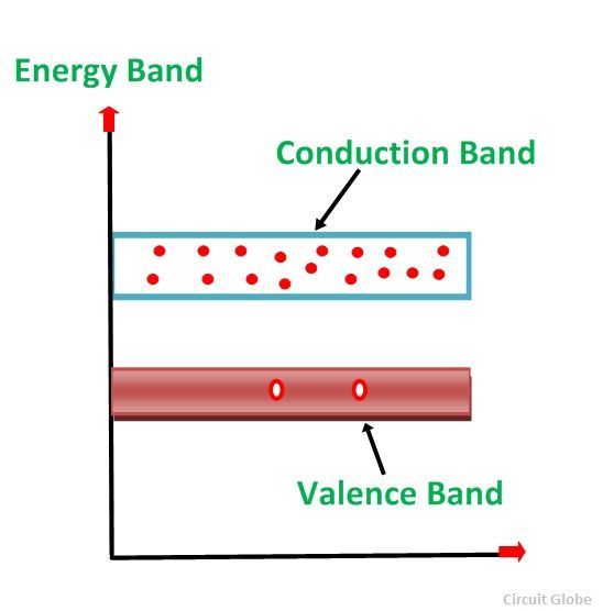
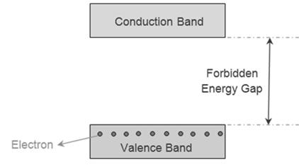
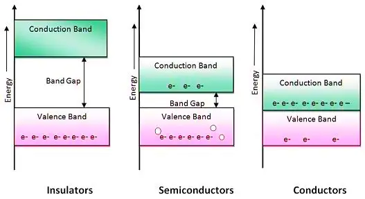
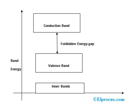
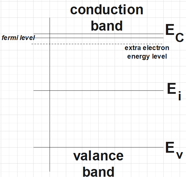
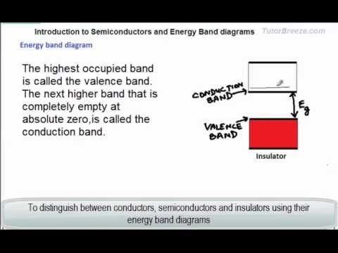
Energy band diagrams for conductor, semiconductor and insulator are shown above. In conductors, both the valance band and conduction band overlap each other. So there is zero band gap in a conductor. In semiconductor, there is a small band gap approximately of 1 e V. In an insulator, there is a large band gap of nearly 5 e V. The figure shows the energy band diagram of the silicon atom. Silicon atom has 14 electrons as silicon atomic number is 14. All 14 electrons are distributed in 3 orbits. All energy level is associated with a certain amount of energy. And all bands are separated from the adjacent bands by the energy gap.No electron can exist in the energy gap. 2. Energy Bands 3. e/h Current Energy Diagrams 21 Energy band diagram shows the bottom edge of conduction band, Ec, and top edge of valence band, Ev. Ecand Evare separated by the band gap energy, Eg. Electrons and holes tend to seek their lowest energy positions, electrons tend to fall in energy band diagram, holes float up like bubbles in water. The energy band diagram of semiconductor is shown where the conduction band is empty and the valence band is completely filled but the forbidden gap between the two bands is very small that is about 1eV. For Germanium, the forbidden gap is 0.72eV and for Silicon, it is 1.1eV. Thus, semiconductor requires small conductivity.
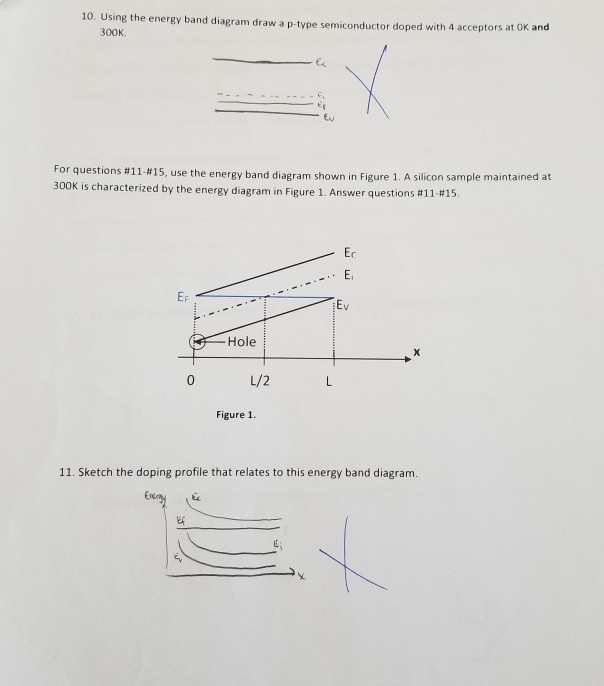
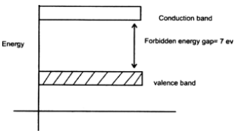
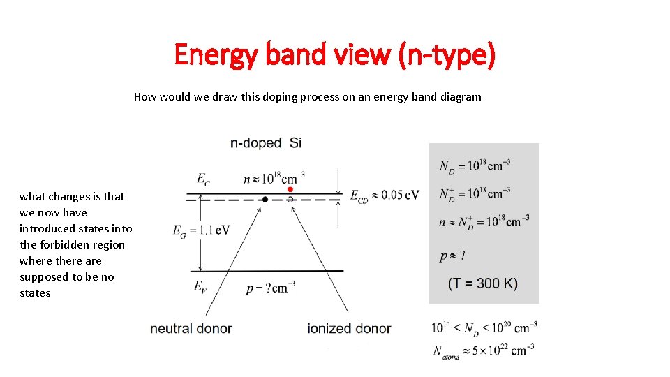
The valance band is full whereas the conduction band is empty as shown in the energy band diagram. The forbidden energy gap between valance band and conduction band is large ( 15 eV ). The electrons of the valance band require very high electric field in order to cross it and move in the conduction band. The energy band diagram of a quantum well is shown in Fig. 1.3a, drawn assuming that the band-bending adjacent to the interfaces occurs over distances much larger than the width of the well and barriers and can be ignored on this scale. The depths of the conduction and valence band wells are determined by the heterostructure band offsets ΔE c, ΔE v which sum to the band gap difference at the ... This program is useful for visualizing approximations of energy band diagrams, and performing back-of-the-envelope calculations of their important parameters. Features: Draw band diagrams for MOS devices in static mode Draw band diagrams for MOS and MIM gate stacks with various dielectrics, including high-κ dielectrics Transcribed image text: Draw the energy band diagrams, showing E_C, E_V, E_ and E_ for the following: assuming all impurities are ionized. a) Intrinsic silicon at 300 K. b) Silicon doped with 10^17 boron atoms cm^-3 at 300K. A silicon sample is doped with 10^16 cm^-3 of phosphorus atoms.
Gallium Arsenide Gaas Energy Band Structure Energy Band Diagram
Semiconductors: The energy band diagram of a semiconductor is similar to that of the insulator but the energy gap is much smaller in the case of semiconductors. The bandgap is less than 3 eV. Typically for Si Eg is 1.1 eV and for Ge, eV is 0.74 eV. Now with the increase in temperature or due to thermal agitation, a large number of electrons ...
What Is N Type Semiconductor Energy Diagram And Conduction Circuit Globe
Draw separate energy band diagrams for conductors, semi-conductors and insulators and label each of them. Answer. Verified. 54.9k+ views. Hint: Understanding about the valence band, conduction band and forbidden band will help to draw the energy band diagram of each material. Conductors don’t have forbidden band gaps.

Draw The Energy Band Diagram Of An Intrinsic Semiconductor Youtube
Band Diagrams (Revisited) E. g. E. C. E. V. Band Diagram Representation. Energy plotted as a function of position. E. C. ÆConduction band. ÆLowest energy state for a free electron. ÆElectrons in the conduction band means current can flow. E. V. ÆValence band ÆHighest energy state for filled outer shells ÆHoles in the valence band means ...
Solved 10 Using The Energy Band Diagram Draw A P Type Chegg Com
In solid-state physics of semiconductors, a band diagram is a diagram plotting various key electron energy levels (Fermi level and nearby energy band edges) as a function of some spatial dimension, which is often denoted x. These diagrams help to explain the operation of many kinds of semiconductor devices and to visualize how bands change with position (band bending).

Band Diagram An Overview Sciencedirect Topics
Drawing energy band diagrams. I'm studying for a course in semiconductor devices, involving pn-diodes, schottky-diodes and mosfet transistors. Just wondering if there's any good online resource that demonstrates specifically how to draw energy band diagrams for the various devices in various situations (applied voltages, inversion, accumulation ...

Draw The Energy Band Diagram Of P N Junction Diode In Forward And Reverse Bias Condition
Indian Institute of Technology Kanpur. In Microsoft work. you can easily draw your energy band diagram with few minute. Follow step: open Microsoft Word..go insert window...shapes.. New Drawing ...
Draw Energy Band Diagram For An Intrinsic Semiconductor At T 0 K Snapsolve
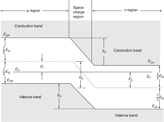
band diagram looks like as shown below. Note that band bending that occurs inside the depletion regions reflecting the presence of an electric field and a corresponding electrostatic potential. Also note that the Fermi level in equilibrium is flat and constant throughout the device. The vacuum level also bends in response to the electric field ...

Energy Band Diagram Revision Ppt Download
Figures 23 and 24 show the energy-band diagram in the region beneath the gate for various HFETs. (The diagrams are labeled for n-type AlGaAs/GaAs devices, but are also applicable to p-type devices and other materials systems.) The simplest structure is the undoped MISFET (or HIGFET) shown in Fig. 23a.As shown, the MISFET consists of a metal gate on an undoped AlGaAs/GaAs heterojunction.

Energy Band Diagram An Overview Sciencedirect Topics
Draw a labelled energy band diagram for a solid which is an insulator. What is the main difference between this diagram and that of a semiconductor? Easy. View solution > In insulator. Easy. View solution > Identify the mismatched pair from the following. Medium. View solution > Assertion
1
Draw band diagrams for MOS devices in static mode; Draw band diagrams for MOS and MIM gate stacks with various dielectrics, including high-κ dielectrics; Show band diagram movement for MOS and MIM devices as gate voltage is swept through a range; Calculate these parameters for applied voltages both in inversion and accumulation regimes: energy

Energy Band Diagram An Overview Sciencedirect Topics
The Answers of Shiromani are absolutely correct. You can use any one software like ATLAS from Silvaco or Sentaurus from Synopsis for the energy band diagram plot. After simulating the structure ...
Simplified Energy Band Diagram Of A P N Junction A At Equilibrium And Download Scientific Diagram
Draw the energy band diagram when intrinsic semiconductor (Ge) is doped with impurity atoms of Antimony (Sb). Name the extrinsic semiconductor so obtained and majority charge carriers in it. class-12; Share It On Facebook Twitter Email. 3 Answers +13 votes . answered Dec 19, 2020 by ...
Material Classification Based On Energy Band Diagram Electricalvoice
The energy band diagrams of semiconductors are rather complex. The detailed energy band diagrams of germanium, silicon and gallium arsenide are shown in Figure 2.3.3. The energy is plotted as a function of the wavenumber, k, along the main crystallographic directions in the crystal, since the band diagram depends on the direction in the crystal. The energy band diagrams contain multiple completely-filled and completely-empty bands.
Draw A Labelled Energy Band Diagram For A Solid Which Is An Insulator What Is The Main Difference Between This Diagram And That Of A Semiconductor From Physics Conductors Insulators And Semiconductors
This quick video will give you a complete analysis of energy band diagram of pn juction diode. This quick video will give you a complete analysis of energy band diagram of pn juction diode.

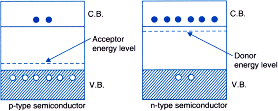
Draw The Energy Band Diagram Of I N Type And Ii P Type Semiconductors At Temperature T 0 K In The Case Of N Type Si Semiconductor The Donor Energy Level Is Slightly Below The Bottom Of Conduction Band Whereas
Energy band diagrams Lundstrom: Fall 2019 An energy band diagram is a plot of the bottom of the conduction band and the top of the valence band vs. position. Energy band diagrams are a powerful tool for understanding semiconductor devices because they provide qualitative solutions to the semiconductor equations.

Draw The Energy Band Diagrams Of A Tunnel Diode Physics
Energy Band Strucure of GaAs. For GaAs, the effective mass of these electrons is 0.067 times the mass of free electron (that is, 0.067m e, where m e is the free electron rest mass). Thus the shapes in the conduction band bring about a superior electron mobility. Due to this, the electrons travel faster in Gallium Arsenide (GaAs) than in Silicon.

Draw The Energy Band Diagrams Of I A Metal And Ii A Semiconductor
Comrades, in this video, we learn about the fabrication of P-N diodes and the Energy band diagram (EBD) of P-N diodes. Here are the timestamps so that you ca...
Draw The Energy Band Diagram When Intrinsic Semiconductor Ge Is Doped With Impurity Atoms Of Antimony Sb Sarthaks Econnect Largest Online Education Community
Pls draw the energy diagram when zero bias is applied to the top electrode. Homework Equations We are taught how to draw the energy diagram for a metal-oxide-semiconductor structure. In this question, we are asked to draw a SOS structure. The Attempt at a Solution

Draw A Labelled Energy Band Diagram For A Solid Which Is An Insulator What Is The Main Difference Between This Diagram And That Of A Semiconductor

1 Sketch Of The Energy Band Diagram At The Metal Semiconductor Download Scientific Diagram

Is There Any Software Available To Draw The Energy Band Diagrams
What Is Energy Band Band Theory And Different Types
Draw The Energy Band Diagrams Of P Type And N Type Semiconductors A Semiconductor Has Equal Electron And Hole Concentration 6 X 10⁸ M 3 On Doping With A Certain Impurity Electron Concentration Increases To 8

Energy Bands Of Silicon Electrical4u
1
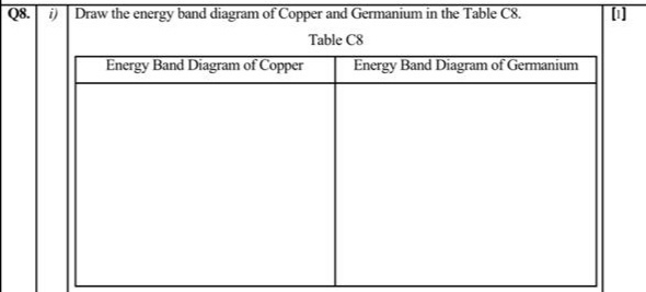
Answered Q8 I Draw The Energy Band Diagram Of Bartleby
Draw Energy Band Diagrams Of An Ntype And Ptype Semiconductor Class 12 Physics Cbse

8 Draw The Energy Band Diagram Of An Unbiased P N Junction And Mark The Barrier Potential And Depletion Region

Draw The Necessary Energy Band Diagrams To Distinguish Between Conductors Semiconductors And Insulators How Does The Change In Temperature Affect The Behaviour Of These Materials Explain Briefly

Is There Any Software Available To Draw The Energy Band Diagrams

Ii Sketch The Energy Band Diagram Of This Doped Material In I At 0 K And Homeworklib

Energy Band Diagram Basics Shortcuts To Draw Any Energy Band Diagram Easiest Method Electronic Youtube

4 Energy Band Diagram Of Simple P N Junction Under Different Operating Download Scientific Diagram
Worldscientific Com
Introduction To Semiconductors And Energy Band Diagrams Youtube

The Energy Band Diagram Of An N Zno P Si Uv Photodiode Under A Download Scientific Diagram
Electronic Devices A Very Brief History Electronic Systems
Tunnel Diode Working And Characteristics Electronics Club

Draw Energy Band Diagram For N Type Semiconductor P Type Semiconductor Physics Semiconductor Electronics Materials Devices And Simple Circuits 9818193 Meritnation Com
Electronic Devices A Very Brief History Electronic Systems

Energy Band Diagram In A Pn Junction All About Circuits

Energy Band Diagram An Overview Sciencedirect Topics
0 Response to "42 how to draw energy band diagram"
Post a Comment