41 phase locked loop block diagram
Describe the basic block diagram of the phase locked loop (PLL). A phase locked loop is basically a closed loop system designed to lock the output frequency and phase to the frequency and phase of an input signal. They are used in applications such as frequency synthesis, frequency modulation/demodulation, AM detection, tracking filters, FSK ... Phase Locked Loop Block Diagram!" ÖN Ref Div Loop Filter VCO Phase Locked Loops (PLL) are ubiquitous circuits used in countless communication and engineering applications. Components include a VCO, a frequency divider, a phase detector (PD), and a loop lter. Niknejad PLLs and Frequency Synthesis
The Phase Locked Loop (PLL) synchronizes a local oscillator with a remote one. This ensures that the local oscillator is at the same frequency and in phase ...

Phase locked loop block diagram
A phase-locked loop or phase lock loop (PLL) is a control system that generates an output signal whose phase is related to the phase of an input signal. There are several different types; the simplest is an electronic circuit consisting of a variable frequency oscillator and a phase detector in a feedback loop.The oscillator generates a periodic signal, and the phase detector compares the ... The phase locked loop or PLL is a particularly useful circuit block that is widely used in radio frequency or wireless applications. In view of its usefulness, the phase locked loop or PLL is found in many wireless, radio, and general electronic items from mobile phones to broadcast radios, televisions to Wi-Fi routers, walkie talkie radios to professional communications systems and vey much more. Phase recovery methods and phase-locked loops. You specify the filter's transfer function in the block mask using the Lowpass filter numerator and Lowpass filter denominator parameters. Each of these parameters is a vector that lists the coefficients of the respective polynomial in order of descending exponents of the variable s.
Phase locked loop block diagram. digital phase locked loop, phase detection is performed by a time to digital converter (TDC), loop filtering is performed by a digital filter, and the oscillator is a digitally controlled oscillator (DCO). PLL Phase Locked Loop: How it Works » Electronics Notes The phase locked loop or PLL is a particularly useful circuit block that is Block Diagram And Working Principle Of PLL. The phase-locked loop consists of a phase detector, a voltage controlled oscillator and, in between them, a low pass filter is fixed. The input signal 'Vi' with an input frequency 'Fi' is conceded by a phase detector. Basically the phase detector is a comparator that compares the input ... Phase Locked Loop System Block Diagram. The figure shows the block diagram of the phase locked loop system in FM transmitter that consists of different blocks such as a crystal oscillator, phase detector, loop filter, voltage controlled oscillator (VCO), and frequency divider. IEEE Press, 1996. Design,"
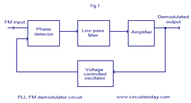
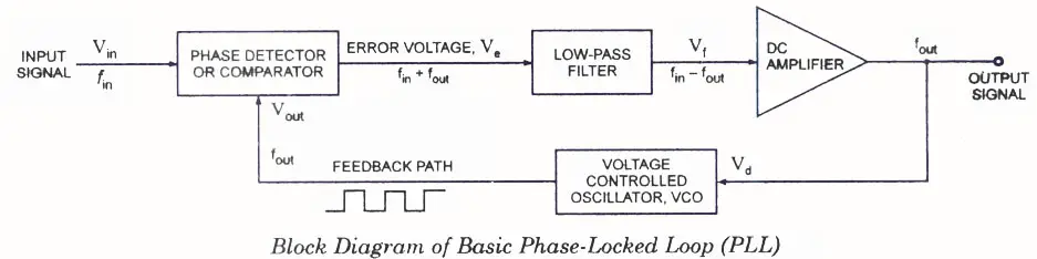
Definition: Phase-locked loops are the circuits used to maintain synchronization between input and output frequency of oscillator circuits by comparing the difference in phase of the two signals.With the evolution of IC, it has emerged as the basic building block of electronic circuits. Phase-locked loops are abbreviated as PLL and are basically a feedback circuit comprising of a phase ... The block diagram of a PLL is shown in fig.1 below. Fig.1: The block diagram of a Phase-Locked Loop (PLL) Working Operation. The operation of a PLL is similar to any other feedback system where the feedback signal tends to follow the input signal. Phase-Locked Loop (PLL) A PLL is a negative feedback system where an oscillator-generated signal is phase and frequency locked to a reference signal. Typical applications of PLL are: Frequency Synthesis (e.g. generating a 1 GHz clock from a 50 MHz reference) Clock Deskewing (e.g. phase-aligning an internal clock to an output clock to external device) Extracting […] LM565 is a general purpose PLL (Phase Locked Loop) IC designed for demodulation, frequency multiplication and frequency division.The device mainly consists of two components, one is voltage controller oscillator and other is phase detector. In which VCO is designed for highly linear operation and PD with good carrier suppression.
Block Diagram of an ADPLL Digital Phase Detector Digital Loop Filter Digital VCO v1 v2' "vd" "vf" Square Waves ... N before M Loop Filter Block diagram: v1 v2' PFD ... When the loop is locked, fc = MNf1. Note that the duration of the start pulse < 1/fc. Waveforms: C. Three-phase PLL design A block diagram displaying the functional components of a generic PLL is shown in Figure 3. For small deviations, standard simplifying assumptions [7] allow the PLL to be modeled according to the linear block diagram of Figure 4, where t is the phase of the measured voltage and p is the phase estimate given by the PLL. A Phase Locked Loop (PLL) is a device used to synchronize a periodic waveform with a reference periodic waveform. It is an automatic control system in which the phase of the output signal is locked to the phase of the input reference signal. In the context of carrier phase synchronization, we talk about tracking the phase of an input reference ... The block diagram of a phase locked loop. (11.35) f ref = f d = F out N. or (11.36) F out = N f ref. Since the divisor N is easy to change in practice, a wide range of frequencies can be generated from a single reference. These frequencies have the accuracy and long-term stability of the original reference.
Basic block diagrams of: (a) conventional phase locked ...
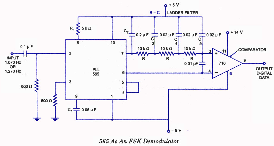
Phase Locked Loop (PLL) is one of the vital blocks in linear systems. It is useful in communication systems such as radars, satellites, FMs, etc. This chapter discusses about the block diagram of PLL and IC 565 in detail. Block Diagram of PLL. A Phase Locked Loop (PLL) mainly consists of the following three blocks −. Phase Detector; Active ...
Software Phase Locked Loop | Hackaday.io
scale:0.85 Continuous time analog phase-locked loop block diagram [ analog_pll_diagram ] depicts a simplified continuous-time analog PLL. We can think of the input to the system as being an unknown phase \(\phi\) , possibly corrupted by noise, while the output of is an estimate of this phase, \(\hat{\phi}\) .

Basic block diagrams of: (a) conventional phase locked ...
The Phase Locked Loop concept was first developed in 1930. Since then it is used in communication systems of different types, particularly in satellite communication system. Before the invention of IC PLL, systems were very complex and costly for use in most consumer & industrial systems.
PLL FM demodulator circuit using XR2212 . Design, working ...
Block diagram: x(t) PFD QA QB VDD Cp I1 I2 S1 S2 VCO y(t) Fig. 2.2-20 The charge pump and capacitor Cp serve as the loop filter for the PLL. The charge pump can provide infinite gain for a static phase shift.
![Activity: The Phase Locked Loop. [Analog Devices Wiki]](http://wiki.analog.com/_media/university/courses/electronics/a31_f1.png?w=600&tok=cae073)
Activity: The Phase Locked Loop. [Analog Devices Wiki]
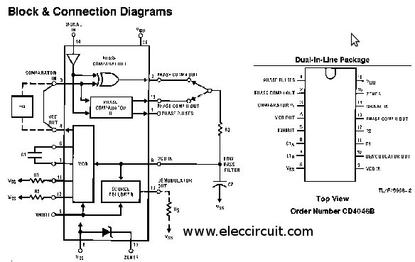
8 CMOS Phase-Locked-Loop Applications Using the CD54/74HC/HCT4046A and CD54/74HC/HCT7046A 92CM-43257 Figure 4. HC/HCT7046A Functional Block Diagram Phase Comparators (PCs) While there are many types of PCs (also referred to as detectors), the ones chosen for the CMOS PLL design are based on accepted industry-standard types. The choice also was ...

Phase Locked Loop Project Overview for Analog Integrated ...
Range of input signal frequencies over which the loop remains locked once it has captured the input signal. This can be limited either by the phase detector or the VCO frequency range. a. If limited by phase detector: π/2 π φ KDπ/2-KDπ/2 Ve 0 < φ < π is the active range where lock can be maintained. For the phase detector type

Phase-locked loop block diagram. | Download Scientific Diagram
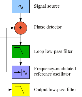
PLL Block Diagram. The block diagram of a basic PLL is shown in the figure below. It is basically a flip flop consisting of a phase detector, a low pass filter (LPF),and a Voltage Controlled Oscillator (VCO). Block Diagram - Phase Locked Loops

Principle block diagram of phase-locked loop. | Download ...
4 CD4046B Phase-Locked Loop: A Versatile Building Block for Micropower Digital and Analog Applications 3 CD4046B PLL Technical Description Figure 2 shows a block diagram of the CD4046B, which has been implemented on a single monolithic integrated circuit. The PLL structure consists of a low-power, linear VCO and two

Phase Lock Loop Design and Construction - Dhruv Patel
In this video i have explainedIntroduction of phase lock loop in hindi. working of phase lock loop. What is Phase Lock Loop (PLL)? How Phase Lock Loop Works....

How to Layout a Phase-locked Loop IC in Your RF PCB | Blog ...
Phase Locked Loop. Phase Locked Loops (PLLs) are feedback control circuits that lock on to the frequency and phase of the input signal and produce an output signal with frequency and phase that is proportional to that of the input. Below is a block diagram of an analog PLL based on a device called a charge pump, which can generate a voltage ...
Phase-locked Loop Modulation Block Diagram Signal, PNG ...
Figure 1 illustrates the block diagram of a phase locked loop. It comprises the following building blocks: Phase-Frequency Detector (PFD) : Outputs a ...

Phase Lock Loop Block Diagram - Atkinsjewelry
The phase locked loop or PLL is an electronic circuit with a voltage controlled oscillator, whose output frequency is continuously adjusted according to the input signal's frequency. A Phase locked loop is used for tracking phase and frequency of the input signal. It is a very useful device for synchronous communication.

Phase-locked loops for high-frequency receivers and ...
This block diagram (and detailed discussion, including SPICE model for closed-loop, time-domain simulations) provide the basic feedback view of operation of the Phase-Locked Loop (PLL) Starting from the input side, the "phase comparator" is the "summing node" (from OpAmp terminology) which generates an

Phase Locked Loop Block Diagram - Hanenhuusholli
Phase recovery methods and phase-locked loops. You specify the filter's transfer function in the block mask using the Lowpass filter numerator and Lowpass filter denominator parameters. Each of these parameters is a vector that lists the coefficients of the respective polynomial in order of descending exponents of the variable s.

06-27-2013: Phase Lock Loop - Demodulation FM and FSK ...
The phase locked loop or PLL is a particularly useful circuit block that is widely used in radio frequency or wireless applications. In view of its usefulness, the phase locked loop or PLL is found in many wireless, radio, and general electronic items from mobile phones to broadcast radios, televisions to Wi-Fi routers, walkie talkie radios to professional communications systems and vey much more.

(PDF) ALL Digital Phase-Locked Loop (ADPLL): A Survey
A phase-locked loop or phase lock loop (PLL) is a control system that generates an output signal whose phase is related to the phase of an input signal. There are several different types; the simplest is an electronic circuit consisting of a variable frequency oscillator and a phase detector in a feedback loop.The oscillator generates a periodic signal, and the phase detector compares the ...

Block diagram of the control system of the DSTATCOM. PLL ...

Optical injection phase-lock loop block diagram. Dotted ...

Phase-locked loop block diagram. | Download Scientific Diagram
IC 4046 datasheet (phase-locked loop)

Linearized Third Order Phase-Lock Loop Block Diagram ...

Phase Lock Loop Block Diagram - Free Diagram For Student

Motor speed control with a phase-locked loop

Phase Locked Loop Tutorial - Block Diagrams - Electronics ...

Phase Locked Loop Block Diagram - Hanenhuusholli

Block diagram of the inverse park transform based phase ...

Reference Clock/Phase-Lock Loop - NI High-Speed Digitizers ...

35 Phase Locked Loop Block Diagram - Wiring Diagram Database

Phase Lock Loop Block Diagram - Diagram Resource Gallery

Block diagram of the phase-lock loop | Download Scientific ...

(PDF) The Design of Phase-Locked-Loop Circuit for ...
* Understanding Phase-Locked Loops

Second order generalized integrator based phase locked ...

The phase locked loop (PLL) block diagram. | Download ...

(PDF) Analysis of Low Power and High Speed Phase Frequency ...

Phase-lock loop: basic block diagram. Deviation of the VCO ...

Control block diagram of the synchronous reference frame ...

Principle block diagram of phase-locked loop. | Download ...

CN0239 Circuit Note | Analog Devices

BLOCK DIAGRAM PHASE LOCKED LOOP | MyCircuits9
PLL-Phase Locked Loops,block diagram,working,operation ...
0 Response to "41 phase locked loop block diagram"
Post a Comment